

- PMBTA42,185 - 分立半导体产品 > 晶体管 > 双极(BJT) > 单双极晶体管
- XC7WH126GD,125 - 集成电路(IC) > 逻辑 > 缓冲器,驱动器,接收器,收发器
- TJA1054AT,518 - 集成电路(IC) > 接口 > 驱动器,接收器,收发器
- MK40DX128VMC7 - 集成电路(IC) > 嵌入式 > 微控制器
- MPXV7007G6U - 传感器,变送器 > 压力传感器、变送器
- PMEG3010BEP,115 - 分立半导体产品 > 二极管 > 整流器 > 单二极管
- SP5745BBK1AMMH2R - 集成电路(IC) > 嵌入式 > 微控制器
- PBRP123ES,126 - 分立半导体产品 > 晶体管 > 双极(BJT) > 单,预偏置双极晶体管
- MPC8360VVAGDGA - 集成电路(IC) > 嵌入式 > 微处理器
- TEF6646HW/V101 - 射频和无线 > 射频接收器
- MC9S12KT256CPVE - 集成电路(IC) > 嵌入式 > 微控制器
- 74HCT7540D,112 - 集成电路(IC) > 逻辑 > 缓冲器,驱动器,接收器,收发器
- LPC1754FBD80,518 - 集成电路(IC) > 嵌入式 > 微控制器
- 74HCT5555D,112 - 集成电路(IC) > 时钟/定时 > 可编程定时器和振荡器
- MMA7341LR1 - 传感器,变送器 > 运动传感器 > 加速计
- MPC564CZP40 - 集成电路(IC) > 嵌入式 > 微控制器
- HEC4538BT,118 - 集成电路(IC) > 逻辑 > 多谐振荡器
- SAF7730HV/N336,557 - 集成电路(IC) > 嵌入式 > DSP(数字信号处理器)
- HEF4046BP,652 - 集成电路(IC) > 时钟/定时 > 时钟发生器,PLL,频率合成器
- AFT26H250W03SR6 - 分立半导体产品 > 晶体管 > FET,MOSFET > RF FET,MOSFET


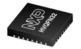
PTN3366BS - Low power HDMI/DVI level shifter with active DDC buffer, supporting 3 Gbit/s operation
PTN3366BS是NXP恩智浦公司的一款高速多路复用器产品,PTN3366BS是Low power HDMI/DVI level shifter with active DDC buffer, supporting 3 Gbit/s operation,本站介绍了PTN3366BS的封装应用图解、特点和优点、功能等,并给出了与PTN3366BS相关的NXP元器件型号供参考。
PTN3366BS - Low power HDMI/DVI level shifter with active DDC buffer, supporting 3 Gbit/s operation - 高速多路复用器 - DisplayPort - 恩智浦
PTN3366 is a low power, high-speed level shifter device which converts four lanes of low-swingAC-coupled differential input signals to DVI v1.0 and HDMI v1.4b compliant open-draincurrent-steering differential output signals, up to 3 Gbit/s per lane to support 36-bitdeep color mode, 4K × 2K video format or 3D video data transport. Each of these lanesprovides a level-shifting differential active buffer, with built-in Equalization, totranslate from low-swing AC-coupled differential signaling on the source side, toTMDS-type DC-coupled differential current-mode signaling terminated into 50 Ω to 3.3 Von the sink side. Additionally, the PTN3366 provides a single-ended active buffer forvoltage translation of the HPD signal from 5 V on the sink side to 3.3 V on the sourceside and provides a channel with active buffering and level shifting of the DDC channel(consisting of a clock and a data line) between 3.3 V source-side and 5 V sink-side. TheDDC channel is implemented using active I2C-bus buffer technology providingredriving and level shifting as well as disablement (isolation between source and sink)of the clock and data lines.
The low-swing AC-coupled differential input signals to the PTN3366 typically come from adisplay source with multi-mode I/O, which supports multiple display standards, forexample, DisplayPort, HDMI and DVI. While the input differential signals are configuredto carry DVI or HDMI coded data, they do not comply with the electrical requirements ofthe DVI v1.0 or HDMI v1.4b specification. By using PTN3366, chip set vendors are able toimplement such reconfigurable I/Os on multi-mode display source devices, allowing thesupport of multiple display standards while keeping the number of chip set I/O pinslow.
The PTN3366 main high-speed differential lanes feature low-swing self-biasingdifferential inputs which are compliant to the electrical specifications of DisplayPortStandard v1.2a and/or PCI Express Standard v1.1, and open-drain current-steeringdifferential outputs compliant to DVI v1.0 and HDMI v1.4b electrical specifications. TheI2C-bus channel actively buffers as well as level-translates the DDCsignals. The PTN3366 supports standby mode in order to minimize current consumption whenHot Plug Detect signal HPD_SINK is LOW.
PTN3366 is powered from a single 3.3 V power supply consuming a small amount of power (72mW typical) and is offered in a 32-terminal HVQFN32 package.
- High-speed TMDS level shifting
- Converts four lanes of low-swing AC-coupled differential inputsignals to DVI v1.0 and HDMI v1.4b compliant open-draincurrent-steering differential output signals
- TMDS level shifting operation up to 3 Gbit/s per lane (300 MHz TMDSclock) supporting 4K × 2K 3 Gbit/s and 3D video formats
- Programmable receive equalization
- Integrated 50 Ω termination resistors for self-biasing differentialinputs
- Back-current safe outputs to disallow current when device power isoff and monitor is on
- Disable feature to turn off TMDS inputs and outputs and to enterlow-power condition
- Selectable differential output termination on TMDS channels
- DDC level shifting
- Integrated DDC buffering and level shifting (3.3 V source to 5 V sinkside and vice versa)
- Rise time accelerator on connector side DDC ports
- Up to 400 kHz I2C-bus clock frequency
- Back-power safe sink-side terminals to disallow backdrive currentwhen power is off or when DDC is not enabled
- HPD level shifting
- HPD non-inverting level shift from 0 V on the sink side to 0 V on thesource side, or from 5 V on the sink side to 3.3 V on the sourceside
- Integrated 200 kΩ pull-down resistor on HPD sink input guarantees‘input LOW’ when no display is plugged in
- Back-power safe design on HPD_SINK to disallow backdrive current whenpower is off
- General
- Power supply 3.3 V
- ESD resilience to 8 kV HBM, 1 kV CDM
- Power-saving modes
- Back-current-safe design on all sink-side main link, DDC and HPDterminals
- Transparent operation: no retiming or software configurationrequired
- 32-terminal HVQFN32 package
- PC motherboard/graphics card
- Docking station
- PMP4501G - NPN/NPN匹配双晶体管
- 74AUP1G97GF - 低功耗可配置多功能门
- PCA9507DP - 适用于HDMI DDC I2C总线和SMBus的2线串行总线扩展器
- 74LVT16646A - 3.3 V 16位总线收发器;3态
- 74ALVCH32973EC - 16位总线收发器和D型透明锁存器,具有8个独立的缓冲区
- PSMN7R0-60YS - N沟道LFPAK 60 V 6.4 m?标准电平MOSFET
- 74AHC139D - 双路2至4线路解码器/解复用器
- BF620 - NPN高压晶体管
- BLF7G22L-200 - LDMOS功率晶体管
- SSL4120T - 集成PFC的谐振电源控制器IC,用于LED照明